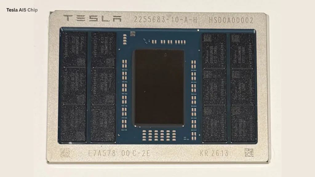
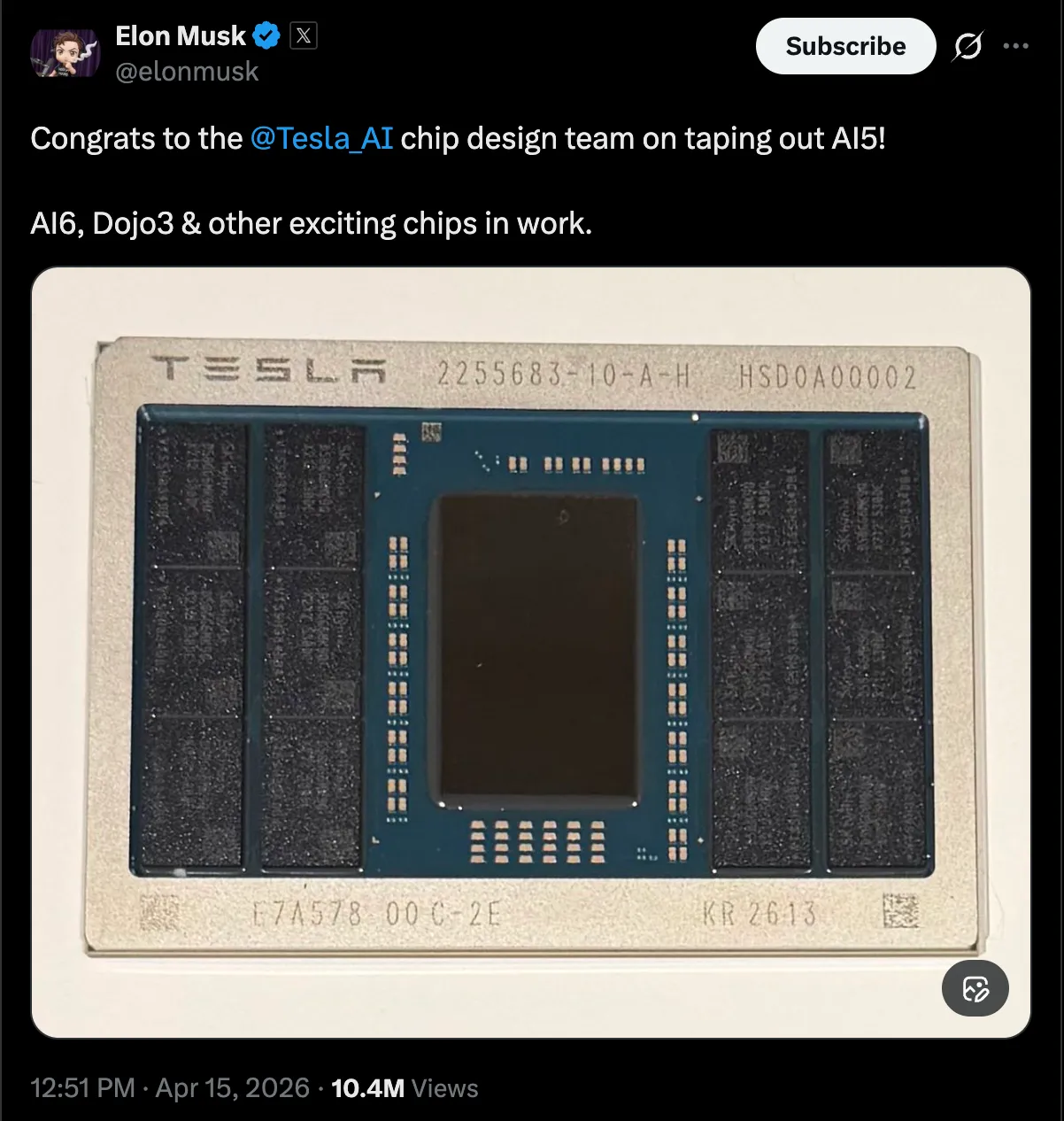
Tesla has finalized the “tape-out” stage for its new AI5 processor, moving the chip from the drawing board to actual manufacturing. In fact, CEO Elon Musk expects this unit to become one of the most widely produced AI chips in history. Eventually, production at scale is planned for 2027. To hit that target, the company partnered with major global foundries for a 2nm manufacturing process.
A new architecture without legacy parts
Engineers took a completely new approach with the AI5 compared to the older Hardware 4. For instance, they adopted a philosophy of “radical simplicity” by dropping traditional components like GPUs and Image Signal Processors. Removing those parts lets the silicon fit into a compact “half reticle” space, and the new setup yields an estimated 2,000 to 2,500 TOPS of computing capacity. Overall, performance metrics reveal a massive leap over older systems.
For example, the chip offers about five times the “useful compute” of a dual-chip AI4 system. It runs certain neural network tasks like Softmax up to 40 times faster natively in one step. Memory capacity grew nine times larger, and memory bandwidth increased to roughly 1.9 TB/s. At the same time, the unit operates at around 250W. A single chip matches the inference speed of an NVIDIA H100, and putting two together rivals a B200 processor at a much lower cost.
Right now, company filings indicate the AI5 will not go into current passenger cars. Musk stated the existing AI4 equipment is good enough to reach safety marks “well beyond human” for standard driving. Instead, the new silicon acts as the “existential” base for heavier tasks. It will run the Optimus Humanoid Robot with real-time reasoning for physical jobs, and it will manage the Dojo 3 supercomputer so Tesla can stop buying external graphics processors.
Later, the hardware will support FSD v15 software. Indeed, that upcoming version relies on large models with around 10 billion parameters. Building a reliable supply chain required deals with both Samsung Electronics and TSMC. Samsung has already made prototypes in Korea using an advanced 2nm process with Gate-All-Around transistors. When 2027 arrives, mass manufacturing will happen in Taiwan, Arizona, and Texas.
Building a massive Texas facility
Tesla announced a 20 billion to 25 billion USD Terafab project at Giga Texas. Today, the massive plant brings chip design, fabrication, and packaging into one building. Intel stepped in to provide advanced 3D stacking and packaging services for the multi-die modules. Next, the AI5 tape-out kicks off an aggressive nine-month release schedule for future processors. Development is already underway on the AI6, which targets double the speed of the AI5.
Looking ahead, engineers are conceptualizing the AI7 for space applications alongside the SpaceX Starlink network. By controlling every layer of the manufacturing process, Tesla removes its dependence on general hardware vendors. Hence, the strategy builds a closed ecosystem focused exactly on the needs of autonomous machines. Analysts say this vertical integration gives the company a massive edge in the coming years.
You may also like to read:
- Tesla to restart Dojo3 after progress on AI5 chip »
- Tesla readies fresh side repeater cameras as AI5 hardware nears »
- Tesla teases AI5 chip to challenge Blackwell, costs cut by 90% »
- Tesla unveils AI5 chip, 40 times faster than AI4 »
We’ve launched an official Tesla Owners Online Forum. Join early and claim your "Founding Fuel" badge.